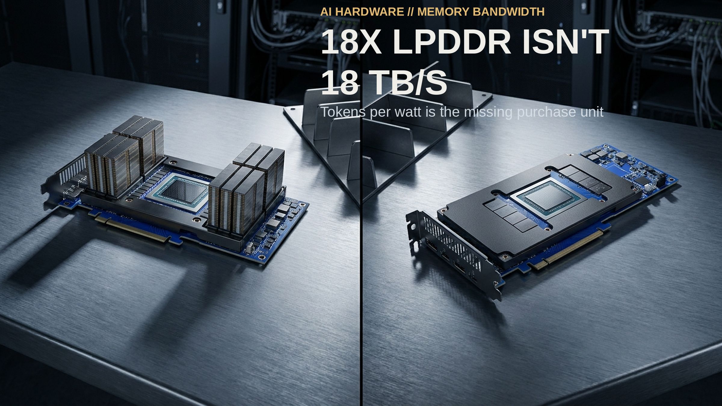
On 2 November, Qualcomm said its first high bandwidth compute (HBC) chip had run a full memory read and write path in the lab. The lab run matters because inference now stalls on data movement rather than arithmetic. The design moves data up to 18 times faster than the low-power memory (LPDDR) it stacks under the compute die [1]. Three weeks earlier, Microsoft put a number on the other approach. Its Maia 300 card moves 18.0 terabytes a second (TB/s) from eight stacks of high bandwidth memory (HBM4) [2]. One is a ratio against a base the other machine does not use, and so 18x LPDDR isn’t 18 TB/s [3].
Two answers to one bottleneck
Both firms start from the same choke point. A language model runs only as fast as its weights can reach the chips, and Microsoft says data movement is that limit rather than raw chip math [2]. From that shared view, the two attack different costs.
Microsoft keeps the stacked memory and widens it. It spends 950 watts per card and a package of several chiplets to reach its rate [2]. Qualcomm removes the stack and changes what sits under it. It bonds a column of LPDDR on top of the die that does the processing, so data travels micrometres rather than millimetres [1][3]. One side buys speed with power and packaging; the other buys it with distance.
Nvidia took a third path. Its custom design moves the memory controller off the graphics chip and into the base die of the stack. The trade press reports this is not an industry standard. Nvidia says it adds up to 30% more bandwidth and frees up to 25% of compute-die area against the standard memory it replaces [4]. Three vendors, three memory designs, three bases for the number on the box.
Then the units break. The Microsoft figure is a rate on one named card, while the Qualcomm claim is a multiple against LPDDR, a base the Microsoft card does not use [3]. I read the two spec sheets side by side and cannot line them up in one column. The shared column would be tokens per watt, but Microsoft names no baseline for its claim and Qualcomm gives no tokens-per-watt figure at all [2][3].
By the numbers
- 27.6 terabytes — memory per rack: a full Maia 300 rack holds 96 cards and 27.6 terabytes of stacked memory. Its 1.7 petabytes a second of total bandwidth sits inside a 167-kilowatt envelope [2].
- 40% — Microsoft tokens-per-megawatt claim: the baseline is “leading GPU-based systems,” with no model, vendor, or test named [2].
- 5x — Qualcomm efficiency estimate: the company puts HBC at five times the terabit-per-second-per-watt of HBM4, measured on lab silicon and normalised to target conditions [3][1].
Where the buyers are stuck
The teams closest to this are not reading spec sheets. They are building the test that will outlive the marketing. Companies that design their own chip can tune it against their own traffic. Microsoft says it did exactly that, feeding what it learned running Maia 200 into the Maia 300 design [2]. Microsoft calls Maia its primary inference system for its own products and services starting in 2027, at multi-gigawatt scale, and the post carries no price and no part number [2].
The Qualcomm path is different. Its lab result is the ticket into design reviews, and the work covered a full read and write path and near-memory math at production sizes. One data center product has taped out, and the Dragonfly AI250 that will carry the design is expected to sample in the first half of 2027 [1]. A merchant chip maker has to prove the lab result first, because its first buyer is a design review, not a fleet.
That leaves the ordinary buyer, a team renting capacity or refreshing a cluster in 2027, reading numbers that were never built to be compared. I keep waiting for someone to publish an outside tokens-per-watt result on a named workload, because that one column would fold three designs into one table. Until then, the honest test remains a team’s own prompt mix, the only test that puts a price on the memory bill.
The shift is already visible in rental pricing, where the cost of an hour on a rented graphics card tracks memory rather than raw processing.
The catch
The tidy story is that these figures are marketing and a buyer should ignore them. I could be wrong, because a ratio is not automatically the weaker claim: if LPDDR supplies the Qualcomm design, then 18x is the right multiple against its own base. What does not survive is the match. It lives only in the Qualcomm footnote, which calls the figures estimates scaled to target conditions that may vary by workload and setup [1].
The same caveat runs the other way. The Microsoft tokens-per-megawatt claim is a forecast for a part that ships in 2027, against a base it declines to name, and no outside test of either part is public [2]. Two vendors can tell the truth and still leave a buyer with nothing to put in a spreadsheet. That is the real state of this market for AI serving this quarter.
At a glance
The shift: The two escapes from the memory wall landed three weeks apart, and one is a speed while the other is a multiple against a different memory. The number: 18.0 TB/s of HBM4 on Maia 300 against 18x LPDDR on the Qualcomm lab chip — two different quantities, not a ranking. The risk: No outside tokens-per-watt result exists for either part, so the only usable test in 2027 is your own workload.
Related reading
- Price of a GPU-Hour Is Now Set by Memory, Not Compute — more on Major Purchases & Assets
- 480GB Won’t Skip Your Memory Queue — more on Major Purchases & Assets
- 1.016M Non-GPUs: Your Chip Stopped Deciding — more on Major Purchases & Assets
Sources
[1] Qualcomm, “Qualcomm HBC demonstrates AI inference leadership with validated silicon”, 2026-11-02 — https://www.qualcomm.com/news/onq/2026/11/qualcomm-hbc-validated-silicon-ai-inference [2] Microsoft, “Microsoft to expand Azure Maia system to multi-gigawatt deployments”, 2026-10-12 — https://blogs.microsoft.com/blog/2026/10/12/microsoft-to-expand-azure-maia-system-to-multi-gigawatt-deployments [3] The Next Platform, “Qualcomm Has Eyes On The AI Inference Datacenter With HBC And AI250”, 2026-11-02 — https://www.nextplatform.com/ai/2026/11/02/qualcomm-has-eyes-on-the-ai-inference-datacenter-with-hbc-and-ai250/5306954 [4] The Register, “Nvidia sidesteps JEDEC HBM standard”, 2026-10-26 — https://www.theregister.com/ai-ml/2026/10/26/nvidia-sidesteps-jedec-hbm-standard/5305323